
The performance of a semiconductor device depends not only on what materials are used, but also on how these materials are arranged. From heterojunctions in conventional semiconductors to artificial superlattices, the ordered stacking of different material layers can reshape electronic band structures and interfacial properties at the nanoscale, enabling optoelectronic functions that are difficult to achieve with a single material. Organic and molecular semiconductors are particularly attractive for constructing heterostructures because their constituents are held together by relatively weak intermolecular interactions and are generally less constrained by stringent lattice-matching requirements. However, unlike inorganic semiconductors, structural design in organic semiconductor films has remained largely at the level of “mixing” rather than “programming.” Different semiconductor materials are commonly blended directly to form bulk heterojunctions, in which donor and acceptor phases spontaneously interpenetrate. Although such structures provide abundant interfaces, it remains difficult to precisely determine where these interfaces are located, in what sequence they occur, or how strongly adjacent layers interact.
In recent years, a range of approaches, including organic molecular beam epitaxy, layer-by-layer solution processing, and interfacial assembly, have been developed to move organic semiconductors from randomly mixed films toward ordered multilayer structures. Yet, constructing organic systems analogous to inorganic superlattices still presents a fundamental challenge: how to insert ultrathin insulating layers of controlled thickness between different semiconductors with molecular-monolayer precision, while freely choosing both the constituent materials and their stacking sequence. Nanoscale dielectric films can serve as interlayers that regulate charge accumulation at interfaces and thereby modify energy-level alignment, providing an additional degree of freedom for semiconductor device design.
To address this challenge, Professor Lei Zhang’s research group has built on its previous work in molecular assembly at the water–air interface and developed a bottom-up assembly strategy with broad material compatibility, enabling organic semiconductor multilayers to be constructed with molecular-monolayer precision. The approach overcomes the conventional requirement for molecular amphiphilicity in Langmuir–Blodgett assembly, allowing different semiconductor polymers to be assembled layer by layer while precisely introducing nanometer-scale dielectric tunnelling layers as thin as approximately 0.6 nm between adjacent semiconductor layers. This enables the construction of organic quasi-superlattices with well-defined stacking sequences and sharp interfaces. By varying the number of molecular layers, material composition, and thickness of the dielectric interlayers, the researchers established clear relationships between multilayer structure and optoelectronic response. Devices based on these programmed architectures achieved light-to-dark signal-to-noise ratios exceeding 106 and could be extended to near-infrared photodetection by replacing the semiconductor components with materials capable of absorbing NIR light. The study demonstrates that performance optimization in organic optoelectronics need not rely solely on conventional material screening and compositional blending. Instead, the spatial arrangement of materials can be programmed from the molecular-layer level, providing a route to organic optoelectronic systems with predefined structures and functions.
The work, entitled “Programmable organic quasi-superlattices with molecular-monolayer precision for enhanced photoconductive response,” has been published in the Journal of the American Chemical Society.
1.Fabrication of a 0.6 nm PVP Nanodielectric Layer
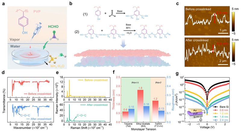
Figure 1. (a) Schematic illustration of the alkali-assisted water-surface self-assembly strategy. (b) Reaction mechanism of vapor-phase formaldehyde crosslinking and schematic structure of the resulting crosslinked PVP. (c) AFM images of island-like PVP monolayers before (top) and after (bottom) base-catalysed crosslinking, showing an unchanged thickness of 0.6 nm. (d, e) FTIR (d) and Raman (e) spectra of PVP films before and after crosslinking. (f) Thickness and root-mean-square (RMS) roughness of PVP layers obtained by compression with different solvents and assembled on neutral or alkaline water. (g) Current density–voltage (J–V) characteristics of Au/PVP/Si devices with varying PVP thicknesses. The PVP layers were crosslinked via base-catalysed phenol–formaldehyde chemistry.
Suppressing dark current has long been a key challenge in improving the performance of organic photodetectors. Conventional approaches often introduce additional carrier-blocking layers near the electrodes to suppress unnecessary background current injection. However, a blocking layer that is too thin can develop leakage pathways through pinholes and defects, whereas an excessively thick layer increases device resistance and impedes the transport of photogenerated carriers. Achieving low leakage without sacrificing carrier transport therefore requires exceptionally precise control over both the thickness and uniformity of the dielectric layer. To address this challenge, the researchers used the water–air interface as a platform for molecular assembly and developed an ammonia-assisted assembly method by introducing ammonia into the aqueous phase. This approach enabled the formation of PVP molecular monolayers with a thickness of only 0.6 nm. Under alkaline conditions, partial deprotonation of PVP promotes the spreading of polymer chains at the water surface, converting PVP from its commonly observed approximately 1.2 nm bilayer structure into a stable monolayer.
The ultrathin molecular layer was subsequently cross-linked in situ through formaldehyde crosslinking reaction. AFM measurements showed that the PVP thickness remained approximately 0.6 nm before and after crosslinking, indicating that chemical reaction did not disrupt the overall monolayer structure. Further spectroscopic characterization confirmed the occurrence of the crosslinking reaction. By varying the solvent used during molecular-layer compression, the number of stacked PVP layers could also be controlled, establishing the 0.6 nm monolayer as the smallest reproducible thickness unit. This provided a precisely tunable nanodielectric platform based on PVP molecular monolayers and laid the foundation for inserting dielectric tunnelling layers between organic semiconductor layers. To evaluate whether the resulting PVP layers were sufficiently compact to function as dielectric tunnelling barriers, the researchers fabricated metal–insulator–metal devices. Increasing the PVP thickness led to a pronounced reduction in leakage current. For a 2.4 nm PVP layer, corresponding to four 0.6 nm monolayers, the leakage current density was only 5 × 10⁻⁴ A cm–2 at 2.5 V, approximately two orders of magnitude lower than that of PVP molecular layers prepared using the group’s previous acid-catalyzed crosslinking method. Notably, even a single 0.6 nm PVP layer exhibited clear dielectric blocking behavior, demonstrating that an ultrathin, compact, and stable molecular layer can serve as an effective tunnelling dielectric.
2.Layer-by-Layer Construction of Organic Heterojunction Photoconductive Devices
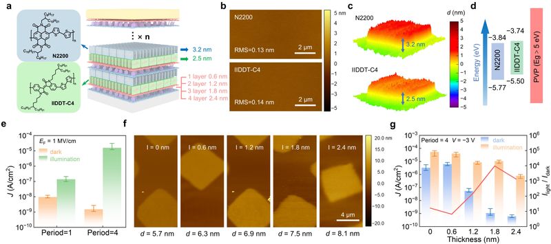
Figure 2. (a) Schematic of the multilayer heterojunction architecture formed by alternating n-type N2200 and p-type IIDDT-C4 monolayers with inserted PVP barriers. (b) AFM images showing molecularly smooth semiconductor monolayers (RMS = 0.13 and 0.14 nm for N2200 and IIDDT-C4, respectively). (c) AFM height profiles of N2200 and IIDDT-C4 monolayers. (d) Electrochemical energy-level diagram of the N2200/IIDDT-C4 heterojunction derived from literature-reported cyclic voltammetry measurements.34,35 (e) Photocurrent and dark current densities for single- and four-period devices. (f) AFM height profiles of multilayer films (IPN×1) with varying PVP spacer thicknesses (I, 0−2.4 nm). (g) Dependence of photocurrent, dark current, and SNR on PVP spacer thickness in four-period devices. Measurements were performed under white-light illumination (Xe lamp, 130 mW cm−2).
With precise control over the subnanometer PVP molecular monolayer established, the researchers then used water-surface-assisted molecular deposition to prepare continuous, fully covered, and transferable monolayers of polymer semiconductors, which could then be sequentially transferred to construct multilayer heterostructures. Using the n-type polymer semiconductor N2200 and p-type polymer semiconductor IIDDT-C4 as the basic building blocks, PVP dielectric layers were selectively inserted between adjacent semiconductor layers, allowing different layer combinations to be assembled in a prescribed sequence and enabling the vertical structure of the organic heterojunction to be programmed at the molecular-layer level. This strategy differs fundamentally from conventional bulk-heterojunction films, in which the spatial distribution of different components is difficult to define precisely. Here, the positions of different materials can be predetermined with molecular-monolayer precision, providing a more controlled route for constructing organic optoelectronic devices. Enabled by the water-surface-assisted molecular deposition (WSAMD) technique developed by the group, both N2200 and IIDDT-C4 formed continuous molecular monolayers. AFM measurements showed that the two semiconductor monolayers had molecular-scale smoothness, with RMS roughness values of only 0.13 and 0.14 nm and thicknesses of approximately 3.2 and 2.5 nm, respectively, consistent with the molecular dimensions of the corresponding polymers.
A key advantage of constructing heterojunctions from polymer monolayers is the extremely short distance that excitons need to travel before reaching the donor–acceptor interface. Because the donor and acceptor are directly adjacent to one another, excitons can reach the heterointerface and undergo dissociation without requiring long-range diffusion. However, the limited thickness of the active absorbing layers in a single-period structure restricts the overall number of photogenerated carriers. The researchers therefore increased the effective absorbing volume by repeating the PN heterojunction unit along the vertical direction. As the number of heterojunction periods increased from one to four, the photocurrent increased substantially. At the same time, the PVP dielectric layers reduced dark current by suppressing transport through the vertical conduction pathway, increasing the device SNR from approximately 10 to approximately 104.
Overall, the multilayer heterojunction architecture assigns different functions to different interfaces with molecular-layer precision. The directly contacting N2200/IIDDT-C4 interfaces promote exciton dissociation and photocarrier generation, while the PVP layers between adjacent periods suppress dark current and regulate carrier transport. Independently tuning these two functions enables a vertically stacked organic heterojunction that combines efficient photocarrier generation and transport with effective suppression of leakage current in the dark. The devices exhibited spectral responses consistent with the absorption spectrum of the active layers and maintained stable and reversible switching over repeated illuminated and dark cycles, demonstrating the structural integrity and optoelectronic stability of the layer-by-layer molecular heterojunctions.
3.Modular amplification and topological programming of organic quasi-superlattices photodetectors
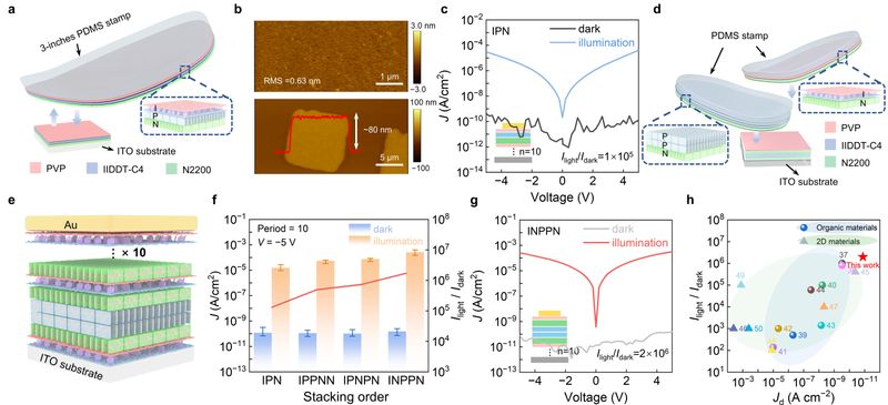
Figure 3. (a) Schematic of the modular transfer-printing strategy, in which preassembled superlattice blocks are sequentially stacked using a PDMS stamp. (b) AFM topography (top) and corresponding height profile (bottom) of a 10-period film (~80 nm thick), showing a smooth surface (RMS roughness 0.63 nm). (c) J−V characteristics of an IPN×10 device in the dark and under 130 mW cm−2 Xe lamp white light. (d) Schematic of a dual-stamp alternating transfer scheme for programmable stacking. (e) Schematic of a photodiode with a centrosymmetric INPPN×10 topology. (f) Statistical comparison of current density and SNR for different stacking sequences (IPN×10, IPPNN×10, IPNPN×10 and INPPN×10). (g) Photoconductive and dark J−V characteristics of the optimized INPPN×10 device, showing the highest SNR (~2 × 10⁶). (h) Benchmark of signal-to-noise ratio and dark current density (Jd). The optimized device (red star) exhibits markedly suppressed dark current compared with both organic and 2D-material photodetectors, while achieving a signal-to-noise ratio among the highest reported across both classes of systems.
To construct quasi-superlattices with a larger number of periods, the researchers developed a PDMS-assisted dry-transfer strategy. PVP, IIDDT-C4, and N2200 molecular monolayers were preassembled on a 3-inch PDMS stamp to form a complete IPN period, which was then multiplied through iterative microcontact printing. This modular approach eliminates the need to repeatedly transfer individual monolayers from the water–air interface and allows the internal structure of each period to be precisely defined on the stamp. After ten lamination cycles, an IPN×10 quasi-superlattice approximately 80 nm thick was obtained with an RMS surface roughness of only 0.63 nm. Its light-to-dark current ratio reached approximately 105, nearly one order of magnitude higher than that of the IPN×4 device. The researchers further used two PDMS stamps to pre-assemble p-type and n-type molecular layers separately, enabling independent control over the stacking topology of the quasi-superlattice. Different structures, including IPPNN×10, IPNPN×10, and INPPN×10, were constructed.
Comparisons showed that increasing the number of absorbing layers within each period, increasing the number of donor–acceptor interfaces, and aligning the same polymer layers across the tunnelling spacer in adjacent periods all contributed to improved photoconductive performance. Among these structures, INPPN×10 delivered the best performance. Under 532 nm illumination, it achieved an SNR of 2 × 10⁶, an ultralow dark current density of 1.3 × 10⁻¹¹ A cm–2, a responsivity of 25 mA W–1, and a specific detectivity of 1.2 × 10¹³ Jones, together with rapid and reversible photo-switching. Compared with organic, two-dimensional-material, quantum-dot, and perovskite photodetectors, the quasi-superlattice device showed particularly strong suppression of background current and enhancement of signal-to-noise performance. Uniform multilayer films over centimeter-scale areas and monolayer transfer over wafer-scale substrates further demonstrated the potential of the PDMS-assisted dry-transfer approach for scalable fabrication.
4.Universality and spectral tunability of organic quasi-superlattices
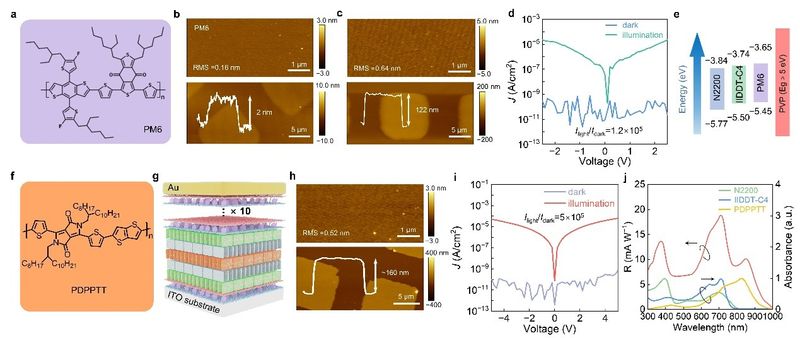
Figure 4. (a) Chemical structure of the donor polymer PM6. (b) AFM topography (top) and height profile (bottom) of a PM6 monolayer. (c) AFM topography of a 10-period PM6-based INPPNI quasi-superlattice (~122 nm thick). (d) J–V characteristics of the PM6-based device, yielding a SNR of 1.2×10⁵.(e)Energy-level alignment of N2200, IIDDT-C4, and PM6. (f) Chemical structure of the narrow-bandgap bipolar polymer PDPPTT. (g) Schematic illustration of a ternary quasi-superlattice architecture incorporating N2200, IIDDT-C4, and PDPPTT layers. (h) AFM topography of the 10-period ternary superlattice. Despite the large thickness (~160 nm), the surface remains molecularly smooth with an RMS roughness of ~0.52 nm. (i) J–V characteristics of the ternary NIR device, maintaining a high SNR of 5×10⁵ for Xe-lamp white light. (j) Spectral responsivity of the ternary device (red line) overlaid with the absorption spectra of the individual components, demonstrating broadband detection extending to 1000 nm.
The researchers next examined the applicability of organic quasi-superlattices across different semiconductor materials and spectral ranges. First, IIDDT-C4 was replaced with PM6 to construct an INPPN×10 structure, allowing the influence of polymer energy-level matching on vertical carrier transport and optoelectronic performance to be examined. The PM6-based device exhibited an SNR of 1.2 × 10⁵, approximately one tenth of that of the IIDDT-C4-based device. This difference is consistent with the shallower LUMO level of PM6 and its larger energy offset relative to N2200, indicating that smoother energy-level variation and a smaller LUMO offset are favorable for electron transport across the stacked layers. The researchers then introduced the narrow-bandgap bipolar polymer PDPPTT into the quasi-superlattice to construct a ternary architecture, INPBPN×10, consisting of N2200, IIDDT-C4, and PDPPTT. Despite increasing the total thickness to approximately 160 nm, the multilayer film retained an exceptionally low RMS roughness of 0.52 nm, with no obvious accumulation of surface roughness during repeated stacking. The ternary device maintained an SNR of 5 × 10⁵ while extending the spectral response to 1000 nm. Its spectral responsivity followed the absorption characteristics of the individual components, demonstrating that the spectral response of organic quasi-superlattices can be tuned by incorporating molecular layers with different optical properties.
5.Organic quasi-superlattices optimized for near-infrared (NIR) detection
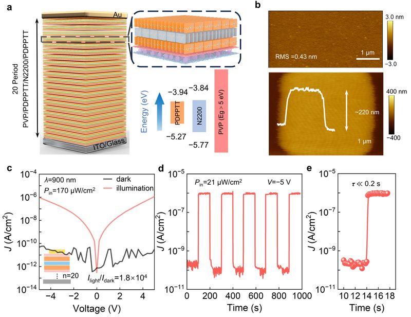
Figure 5. (a) Schematic illustration of the 20-period superlattice architecture designed for NIR photodetection, consisting of repeating PVP/PDPPTT/N2200/PDPPTT units. The inset shows the corresponding energy-level diagram with the type-I band alignment between PDPPTT and N2200. (b) AFM topography (top) and height profile (bottom) of the 20-period film. (c) J-V characteristics under 900 nm illumination (170 µW cm−2), yielding an average light-to-dark current ratio of 1.8×10⁴. (d) Transient photoresponse under ultralow NIR irradiation (21 µW cm−2), exhibiting stable switching behaviour with an on/off ratio approaching 104. (e) Magnified view of the photocurrent rising edge extracted from the transient response measurements.
Because the performance enhancement becomes increasingly limited as the number of molecular layers increases in each period, the researchers further optimized the quasi-superlattice architecture for NIR detection. By comparing the energy-level matching of different semiconductor monolayers, the combination of N2200 and PDPPTT was identified as the most favorable for photoconduction. A 20-period IBNB×20 quasi-superlattice was then constructed from repeating PVP/PDPPTT/N2200/PDPPTT units. Despite a total thickness of approximately 220 nm, the multilayer structure retained a subnanometer surface roughness of only 0.43 nm. Under 900 nm illumination, the device achieved an ultralow dark current density of 3.1 × 10⁻¹¹A cm–2, a photocurrent density of 1.1 × 10⁻⁶ A cm–2, a responsivity of 6.47 mA W–1, a peak light-to-dark current ratio exceeding 3.5 × 10⁴, and a specific detectivity of 2.06 × 10¹² Jones. Unlike conventional organic photodiodes, which often rely on rectification to suppress leakage current, the quasi-superlattice primarily uses molecularly thin PVP tunnelling barriers to regulate interlayer charge transport, while the donor–acceptor heterojunctions promote exciton dissociation and photocarrier generation. Under ultralow NIR illumination of only 21 μW cm–2, the device still exhibited stable photo-switching with an on/off ratio of 103–104. Transient measurements showed that the switching process was faster than the 0.2 s temporal resolution of the measurement. Further measurements with a temporal resolution of 35 ms showed that the device could complete the switching process within a single sampling interval, suggesting that its intrinsic response is likely substantially faster than the current measurement resolution.
6. Conclusion and Outlook
In this work, the research team established a molecular-layer-based route for constructing organic quasi-superlattices with controlled stacking sequences and well-defined interfaces. The approach addresses the interlayer intermixing that commonly complicates multilayer organic semiconductor structures and enables the fabrication of vertically stacked architectures with molecular-monolayer precision. Within these structures, the approximately 0.6 nm PVP molecular layer serves as an effective tunnelling dielectric. It suppresses dark current while still allowing photogenerated carriers to pass through the multilayer structure, helping reconcile the competing requirements of electrical insulation and carrier transport in organic photodetectors. At the same time, the quasi-superlattice retains the short exciton diffusion distance associated with molecular-layer heterojunctions while increasing the amount of light-absorbing material through repeated stacking. The resulting devices show high light-to-dark current ratios and detectivity in both the visible and near-infrared regions. Even after approximately 20 periods are stacked to reach a total thickness of around 220 nm, the films retain subnanometer-scale surface smoothness, with no pronounced buildup of roughness during stacking. This behavior is consistent with a strain-free, van der Waals-like multilayer configuration.
Although the glassy and amorphous character of polymer molecular layers makes their nanoscale structural characterization intrinsically less definitive than that of crystalline two-dimensional atomic materials, AFM thickness measurements nevertheless show highly reproducible layer-by-layer growth, with the measured total thickness closely following the expected value based on the monolayer thickness and the number of stacked periods. More broadly, this work provides a different way of thinking about the design of organic optoelectronic materials. Rather than relying primarily on material selection and compositional blending, the properties of the device can be engineered by deliberately defining how different molecular layers are positioned and connected. This molecular-level structural programming provides a scalable foundation for flexible organic optoelectronics and spectrally tunable photodetection, with potential applications in multiband and hyperspectral imaging.