
With the rapid development of machine learning and other artificial intelligence technologies, the separation of memory and computation in the conventional von Neumann architecture is facing increasingly severe challenges. This is driving electronic information technology toward new device architectures with highly integrated functions, such as memristors and in-memory computing. For next-generation information storage, memory materials need to simultaneously meet multiple requirements, including non-volatility, high integration density, ultralow power consumption, fast response, and multilevel state switching, while also enabling effective integration with logic and sensing functions. To address these demands, researchers have developed a variety of emerging nanomaterials for information storage. Among them, molecular materials offer unique advantages. For example, their dimensions are intrinsically defined by their chemical structures, allowing them to reach the nanoscale naturally, while their optoelectronic and physicochemical properties can be precisely tailored through molecular design. More importantly, molecules can respond to a wide range of external stimuli, including electrical, optical, thermal, mechanical, and chemical inputs. These characteristics make molecular materials promising candidates for highly tunable and multifunctional molecular electronic and optoelectronic systems, particularly in flexible electronics and complex heterostructure devices.
However, converting the rich reversible state changes of molecules into reliable and integrable device-level resistive switching remains an important challenge. Specifically, molecules can undergo multistate transformations through mechanisms such as conformational changes, dipole switching, photoisomerization, controlled doping, and charge trapping and release. Yet how these molecular-scale changes can be reliably and efficiently programmed and read, and further exploited for multibit storage and logic-memory integration, remains challenging. Early studies mainly employed vertical metal/molecule/metal structures to achieve binary resistive switching. Although structurally simple, these devices use the same current pathway for both programming and readout, making effective spatial separation difficult and limiting the development of more complex functions such as multilevel storage and logic-memory integration. Metal-insulator-semiconductor field-effect transistors subsequently introduced gate modulation, enabling independent control of the memory state while providing signal amplification. However, compared with diode-based crossbar architectures, their structures are more difficult to miniaturize. Moreover, the electric field in transistor channels is inherently non-uniform, and manipulation of minority carriers often requires optical assistance. Another class of molecular memories based on scanning tunneling microscope probes can achieve extremely high storage densities, but their limited addressability makes large-scale integration difficult.
To address these challenges, Professor Lei Zhang’s research group was inspired by the unidirectional convergence of fluid in a funnel and proposed a novel “funnel diode” device architecture. This architecture combines several important advantages, including compact device dimensions, rectification, gate modulation, a uniform internal electric field, and low-voltage operation. The device consists of a high-quality polymeric nanodielectric layer only 3.6 nm thick and decorated with periodic nanopores, together with a 10–30 nm-thick p-type organic semiconductor, pentacene, sandwiched between top and bottom electrodes. Under forward bias, the nanopores act as “current funnels” that guide carrier transport, while the gating effect of the dielectric layer further concentrates majority-carrier injection, resulting in a rectification ratio exceeding 104. Building on this architecture, the research group further incorporated molecular monolayers as active memory layers using its previously developed Solvent Surface Tension Balance (SSTB) and Water-Surface-Assisted Molecular Deposition (WSAMD) techniques. By inserting either a copper stearate molecular monolayer or an Au25(SR)18 nanocluster monolayer between the dielectric and semiconductor layers, the researchers realized nonvolatile memory and synaptic plasticity functions, respectively. Overall, the funnel diode provides a general device architecture for memristive switching based on atomically or molecularly thin interfacial storage layers, enabling bidirectional low-power programming and nondestructive readout. Meanwhile, the signal amplification arising from gate modulation allows operation at readout voltages as low as ±0.05 V, opening new possibilities for neuromorphic computing, high-density information storage, and post-Moore information-processing systems.
The work, entitled “A Funnel Diode Enabled by Nanopores-Decorated Dielectric Polymer Monolayer for Integrated Field-Effect Gating, Rectification, and Memristive Switching,” was published in the Journal of the American Chemical Society: (Link: https://doi.org/10.1021/jacs.5c15078)
1.Fabrication of the funnel diode.
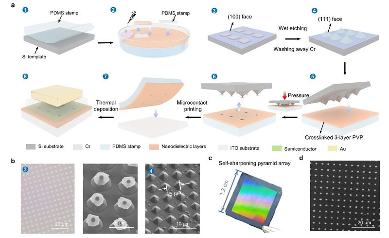
Figure 1.(a) Schematic illustration of the fabrication process for the funnel-shaped diode. (b) Self-sharpening formation of the pyramid array via anisotropic wet etching. From left to right: optical image of a Cr square array patterned by photolithography; SEM image of partially etched pyramidal structures; SEM image of a fully developed pyramid array after Cr removal. (c) Photograph of a highly periodic pyramid array displaying a distinct optical diffraction pattern arising from grating effects. (d) SEM image of the polymeric nanodielectric layer with uniformly distributed nanopores.
The key functional component in funnel diodes is a polymeric nanodielectric layer (PNDL), fabricated using the group’s previously developed poly(4-hydroxystyrene) (PVP) molecular monolayer technology. The researchers first assembled and compressed PVP molecular monolayers at the water surface, then transferred and stacked them layer by layer to form an ultrathin dielectric layer consisting of three PVP monolayers, with a total thickness of approximately 3.6 nm. Subsequent dual crosslinking with formaldehyde and SiCl4 endowed the ultrathin polymer dielectric with excellent dielectric properties comparable to those of HfO2 dielectric layers prepared by atomic layer deposition. The three-layer PVP dielectric was then transferred onto a PDMS stamp. By bringing it into contact with a sharp-tipped silicon pyramid array under precisely controlled pressure, regularly distributed nanopores were introduced into the polymer dielectric layer.
As the key structural template of the funnel diode, the silicon pyramid array was fabricated by anisotropic wet etching of silicon, without relying on costly nanofabrication techniques such as electron-beam lithography or focused ion beam etching. A chromium hard mask was used to control the etching process, producing high-resolution pyramid arrays with tip dimensions below 50 nm. The arrays exhibited excellent uniformity over centimeter-scale substrates and could be reused. The periodicity of the pyramid array determined the periodic arrangement of nanopores in the polymer dielectric. By modifying the pattern of the chromium mask, the periodicity of the nanopore array could also be flexibly adjusted, providing control over the structural parameters of the funnel diode.
2.Rectifying behavior and working mechanism of the funnel diode.
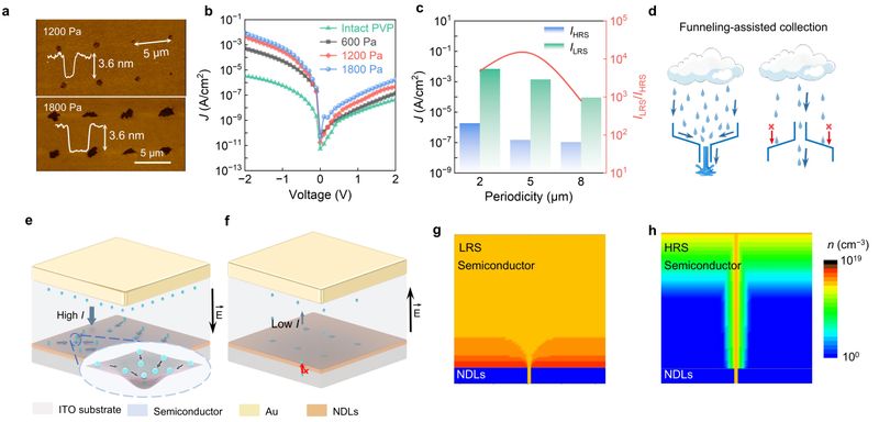
Figure 2. (a) Atomic force microscopy (AFM) images of nano-dielectric layers with nanopores of varying sizes, obtained under different contact pressures. (b) Current density–voltage (J–V) curves and rectification behavior of funnel diodes with pressure-induced nanopores of different sizes.The top electrode was grounded (0 V) during diode testing. (c) Forward and reverse current densities measured from devices with varying nanopore periods. (d) Schematic cartoon illustrating the unidirectional current collection enabled by the funnel geometry. (e, f) Schematic diagrams of the rectification mechanism under low-resistance and high-resistance states, respectively. (g, h) Two-dimensional numerical simulations of charge carrier distribution using Technology Computer-Aided Design (TCAD) under forward and reverse bias voltages, respectively.
The researchers controlled the nanopore size by adjusting the contact pressure between the PDMS stamp and the silicon pyramid array. Higher contact pressure produced larger nanopores, enabling flexible control over the nanostructure of the funnel diode and providing an additional degree of freedom for device optimization. The nanopore-patterned polymer nanodielectric layer was subsequently transferred onto a flat, transparent indium tin oxide (ITO) electrode. The transparent electrode allowed the device to be illuminated when required, providing a platform for subsequent photo-assisted measurements. A pentacene semiconductor layer and a gold top electrode were then sequentially deposited by thermal evaporation to complete the funnel diode. Current density–voltage (J–V) measurements showed that the size of the nanopores had a significant influence on rectification. Among devices fabricated under different contact pressures, those prepared at 1200 Pa exhibited the best rectifying performance, with an average nanopore diameter of approximately 200 nm.
Further variation of the nanopore periodicity revealed that increasing nanopore density enhanced both the forward and reverse current densities. The highest rectification ratio, approximately 1.4 × 10⁴, was achieved with a nanopore periodicity of 5 μm. These results demonstrate that the transport properties of the funnel diode can be effectively optimized by controlling both nanopore dimensions and their spatial density. Because neither the gold nor ITO electrode forms a strongly rectifying contact with pentacene, the excellent rectification does not originate from conventional metal–semiconductor contact effects. Instead, it arises from the asymmetric nanostructure and the gate-modulation effect of the polymer nanodielectric layer. The working principle resembles the unidirectional convergence of fluid through a physical funnel. Under forward bias, the electric field is directed from the top electrode toward the bottom electrode, allowing majority carriers to be efficiently injected into the pentacene semiconductor and accumulate near the pentacene/polymer dielectric interface. These carriers then diffuse laterally along the interface before converging through the nanopores toward the bottom electrode, producing a low-resistance state (LRS).
Under reverse bias, the high-quality polymer dielectric effectively suppresses carrier injection, restricting transport primarily to the nanopore regions and substantially reducing the overall current. The device therefore enters a high-resistance state (HRS). To further verify this funneling mechanism, the researchers performed two-dimensional numerical simulations using Technology Computer-Aided Design (TCAD) to analyze the carrier concentration distributions under forward and reverse bias. The simulation results were consistent with the experimental observations, further supporting the proposed mechanism of unidirectional carrier convergence enabled by the nanopore structure and interfacial gate modulation.
3.Preparation and characterization of molecular monolayers as memory components.
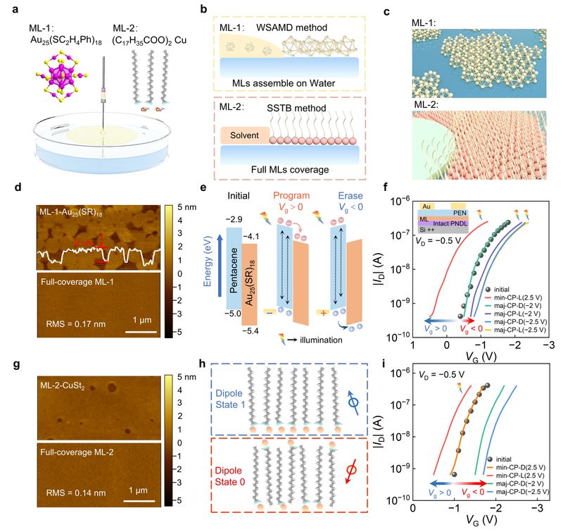
Figure 3. (a) Schematic of the monolayer fabrication process. (b) Conceptual diagrams of the WSAMD and SSTB approaches. (c) Schematic depiction of Au nanocluster and stearic acid molecules monolayers floating at the air-water interface. (d) AFM image of the Au nanocluster monolayer: upper part shows partial coverage as prepared by WSAMD; lower part shows full coverage after compression by SSTB. (e) Schematic of the charge trapping mechanism in Au nanocluster-based memory being coupled with pentacene. (f) Memory window characteristics of bottom-gate, top-contact transistors incorporating Au nanocluster monolayers. In this device, an intact PVP nanodielectric (three layers, ~3.6 nm, dual-crosslinked) served as the gate insulator (see inset). Min-CP and Maj-CP demote minority and majority carrier polarization, respectively; L and D indicate light-assisted and dark conditions. (g) AFM images of copper stearate monolayers: nearly complete coverage with minor defects (top) and full coverage (bottom). (h) Schematic of the dipole-switching mechanism in copper stearate memory monolayer. (i) Memory window characteristics of OFET employing copper stearate monolayer under Min-CP and Maj-CP conditions.The device architecture was identical to that shown in Figure3f.
The current in the LRS of the funnel diode is primarily governed by the gating effect of the polymer nanodielectric layer. Therefore, introducing a molecular monolayer with memory functionality onto the PVP dielectric layer allows the funnel diode to acquire memory characteristics analogous to those of a memory OFET. At the same time, the funnel architecture provides more concentrated carrier transport and a more uniform internal electric field, potentially enabling lower-voltage memory programming. The researchers selected two representative molecular memory materials: the gold nanocluster Au25(SC2H4Ph)18 and copper stearate. Using the previously developed SSTB and WSAMD techniques, these water-insoluble materials were assembled at the water–air interface into large-area, continuously covered molecular monolayers and subsequently transferred onto device substrates. At the water–air interface, Au25(SC2H4Ph)18 nanoclusters initially formed island-like structures with a thickness of approximately 2 nm.
Compression using a mixed solvent of toluene and ethyl acetate caused these separated islands to gradually merge into a continuous, compact, and highly smooth molecular monolayer, with a root-mean-square roughness as low as 0.17 nm. This result demonstrates that SSTB and WSAMD can effectively enable large-area assembly and uniform coverage of molecular nanoclusters in monolayer form. Based on the energy-level relationship between the gold nanoclusters and pentacene, the researchers attributed the memory behavior primarily to electron and hole trapping by the gold nanoclusters. To verify this mechanism, they first fabricated organic field-effect transistors incorporating the gold nanocluster monolayer as the memory layer. The experiments showed pronounced and reversible threshold-voltage shifts under different polarization conditions, demonstrating that the molecular monolayer could effectively store charge and establish distinct interfacial memory states.
Copper stearate exhibited a fundamentally different memory mechanism. Because stearic acid is amphiphilic, it can spontaneously form a stable molecular monolayer at the water surface. Further interfacial compression using SSTB transformed the initially nearly complete layer into a highly dense and smooth continuous film, with an RMS roughness below 0.14 nm. Unlike the charge-trapping mechanism of gold nanoclusters, the copper stearate molecular monolayer may operate through an electret-like mechanism. Molecular dipoles formed through coordination between copper ions and long-chain fatty acids can undergo reversible reorientation under an external electric field, generating different polarization states and memory windows. Experiments further showed pronounced threshold-voltage shifts and stable nonvolatile memory characteristics in copper stearate memory OFETs under different polarization conditions.
Importantly, although the two molecular monolayers rely on different memory mechanisms, both can be effectively integrated with the nanostructured dielectric architecture of the funnel diode. This demonstrates that molecular monolayers can serve as independent active storage units, carrying information states through mechanisms such as charge trapping or molecular dipole reorientation. At the same time, the concentrated electric field and gate-modulation effect provided by the funnel diode offer an efficient electrical pathway for controlling and reading these molecular-scale state changes, providing a foundation for low-power molecular memory devices.
4.Storage performance of the funnel diode.
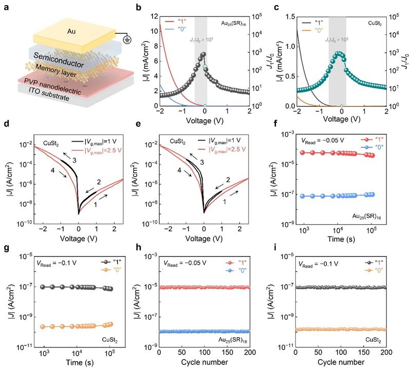
Figure 4. (a) Schematic diagram of the memory device structure based on the funnel diode and molecular monolayer (e.g., Au nanoclusters). (b, c) J–V curves and readout windows for the “0” and “1” states of funnel diodes incorporating monolayers of gold clusters (b) and copper stearate (c), respectively. (d, e) Ferroelectric-mimicking hysteresis loops of copper stearate monolayers in funnel diode memory devices with pentacene layer thickness of 30 nm (d) and 10 nm (e), respectively.The numbers “1–4” indicate the scanning sequence during the J–V measurement, with scans 1 and 2 corresponding to the programming process (switching from the “0” to the “1” state) and scans 3 and 4 corresponding to the erase process (resetting). The observed counterclockwise loop during programming scans indicates pseudo-ferroelectric behavior. (f, g) Data retention characteristics of funnel diode memory devices based on gold cluster monolayers (f) and copper stearate monolayers (g). (h, i) Endurance performance of funnel diode memory devices incorporating gold cluster monolayers (h) and copper stearate monolayers (i).
After successfully fabricating the gold nanocluster and copper stearate molecular monolayers and establishing their respective memory mechanisms, the researchers integrated both molecular storage layers into the funnel diode architecture to construct molecular memory devices. For the gold nanocluster funnel diode, programming was achieved by applying +2.5 V or −2.5 V for 10 seconds, with optical assistance required during positive-bias programming. After programming, the two memory states exhibited well-defined low-voltage readout windows. At a readout voltage of −0.05 V, the current ratio between the two states exceeded 103, while a maximum ratio of approximately 102 was obtained at +0.05 V. This asymmetry originates from the field-effect rectification characteristics of the funnel diode. Under negative bias, the device enters its forward-conduction regime, where holes accumulated at the pentacene/polymer dielectric interface become more sensitive to the stored molecular state, producing a larger electrical contrast.
The copper stearate funnel diode also exhibited clear discrimination between the “0” and “1” states. Using a current ratio above 102 as the criterion for reliable state discrimination, the device provided a low-voltage readout window spanning approximately −0.6 to +0.2 V. More importantly, unlike conventional OFET-based memory devices, both polarization processes in the copper stearate funnel diode could be achieved without optical assistance and through purely electrical control. This advantage arises from the vertically stacked parallel-plate electrode configuration, which generates a uniform and highly confined electric field across the molecular memory interface, efficiently driving molecular dipole reorientation. Under dark conditions, the device exhibited a pronounced ferroelectric-like hysteresis behavior when swept between 0 and 2.5 V. Because polarization switching depends primarily on electric-field strength, the hysteresis disappeared at lower voltages such as ±1 V. However, when the pentacene thickness was reduced from 30 nm to 10 nm, a well-defined hysteresis loop emerged even under ±1 V voltage sweeps.
This result indicates that further optimization of the funnel diode geometry and materials could enable even lower operating voltages and energy consumption. The researchers further evaluated the memory window, data retention, and cycling stability. Both gold nanocluster- and copper stearate-based devices exhibited resistance ratios between the “0” and “1” states of approximately 102–103, sufficient for reliable state discrimination under low-voltage readout. After 105 seconds of storage, both devices retained an on/off ratio above 102, demonstrating robust nonvolatile characteristics. In addition, after 200 repeated programming/erasing cycles, the memory window remained essentially unchanged, demonstrating good cycling durability and operational repeatability.
5.Funnel diode based on gold cluster monolayers for artificial synapses.
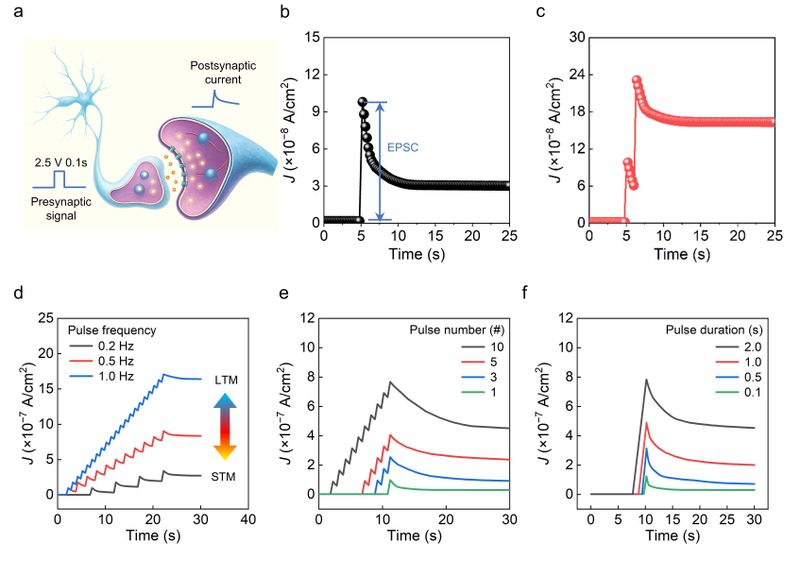
Figure 5. (a) Schematic illustration of a biological synapse. (b) EPSC (Excitatory Post-Synaptic Current) triggered by a single voltage pulse. (c) EPSC response to a pair of voltage pulses with the Δt of 0.1 s. (d–f) STM-to-LTM transition processes induced by modulating the (d) pulse frequency, (e) pulse number, and (f) pulse duration of presynaptic voltage.
Beyond conventional information storage, the gold nanocluster funnel diode also exhibited voltage-response and photoresponse characteristics, making it suitable for emulating artificial synapses and learning-related behaviors. Under illumination, pulsed voltage stimulation induced the accumulation of photogenerated carriers within the gold nanocluster molecular monolayer, producing an electrical response analogous to an excitatory postsynaptic current (EPSC) in biological synapses. A single presynaptic voltage pulse generated a distinct EPSC response, reaching a peak current density of approximately 100 nA cm–2 at the end of the pulse and gradually decaying to approximately 30 nA cm–2 over 20 seconds. This transient response resembles the excitatory response of biological synapses following stimulation.
When two identical voltage pulses were applied consecutively, the second pulse generated a substantially larger EPSC than the first, demonstrating the characteristic paired-pulse facilitation (PPF) phenomenon, an important form of short-term synaptic plasticity. The researchers further investigated the transition from short-term memory (STM) to long-term memory (LTM) by varying the frequency, number, and duration of presynaptic voltage pulses. Higher stimulation frequencies, larger numbers of pulses, longer pulse durations, and stronger pulse amplitudes produced stronger EPSC responses and slower decay dynamics. This behavior resembles memory consolidation induced by repeated rehearsal in biological neural networks, providing preliminary evidence for the potential use of gold nanocluster funnel diodes in neuromorphic computing and brain-inspired information processing.
6.Summary and Outlook
This work introduces a new funnel diode architecture that incorporates the gate-controlled signal amplification and functional tunability of field-effect devices into a compact vertical diode structure, while addressing some of the limitations of conventional transistors in miniaturization, electric-field uniformity, and operating voltage. Its compact architecture also offers potential for high-density integration in configurations analogous to crossbar diode arrays. By combining this architecture with SSTB and WSAMD molecular-monolayer fabrication technologies, the researchers demonstrated that molecular materials with distinct storage mechanisms, including gold nanoclusters and copper stearate, can be integrated into funnel diodes to realize nonvolatile memory with low-voltage programming and readout. The gold nanocluster funnel diode further demonstrated key synaptic functions, including EPSC, PPF, and the transition from short-term to long-term memory under repeated stimulation, highlighting the possibility of extending molecular memory toward neuromorphic computing.
More broadly, the platform is not limited to these two molecular systems. Molecular monolayers offer highly designable chemical structures and diverse physicochemical response mechanisms, making it possible to introduce functional molecules responsive to electrical, optical, thermal, or chemical stimuli and directly translate molecular-scale state changes into measurable electrical signals. In the future, further optimization of the molecular monolayers, dielectric quality, and nanostructured dielectric geometry—including nanopore size, periodicity, and thickness—could further improve device performance and enable the integration of memory, sensing, and computing functions within a single platform. Therefore, the funnel diode provides a new platform for exploiting molecular-scale functional units to construct high-density, low-power, and multifunctional information-processing hardware, offering a potential new device architecture for artificial intelligence, machine learning, and neuromorphic electronics.